
High-performance Thick copper heavy Copper PCB 6Oz 10Oz 20Oz
Views : 179
Author : Meidear
Update time : 2024-08-09 09:32:17
With the continuous development of electronic technology, the requirements for the current conductivity and load-bearing capacity of printed circuit boards (PCBs) are also increasing. Thick copper PCB, also known as PCB with thicker copper foil, is commonly used in industrial automation, power electronics, automotive electronics, power systems and other fields because they require better current carrying capacity and thermal management capabilities. However, the production process of thick copper PCB is more complex than standard PCB and faces various production difficulties. This article will provide a detailed analysis of these difficulties.
1. Material selection and processing difficulty
The production of thick copper PCB first faces the problem of material selection. The increase in thickness of copper foil means that the hardness and stiffness of the material will also increase, which poses challenges for subsequent processing. Meanwhile, thick copper plates require longer chemical treatment during the etching process, which not only increases production costs but also raises the requirements for process control.

2. Increased difficulty in drilling
Drilling is a key technical step in the PCB manufacturing process. For thick copper PCB, due to the thicker copper layer, greater torque and thrust are required during drilling, which can easily lead to accelerated wear and even fracture of the drill bit. In addition, thick copper plates generate more heat during the drilling process, which can easily cause rough hole walls or burr formation, affecting the quality of PCBs Drilling difficulty increases.

3. Copper plating uniformity challenge
Ensuring the uniformity of the copper layer on the entire surface of thick copper PCB during electroplating is a challenge. Due to the thick copper layer, the distribution of electroplating solution on the surface of the board may be uneven, resulting in inconsistent thickness of the copper layer. This non-uniformity can affect the performance of the circuit, especially in high-frequency applications.
4. Dimensional stability control
As the thickness of the copper layer increases, the thermal expansion and contraction phenomena of the PCB during heating and cooling become more pronounced. This requires strict control of temperature changes during the production process to ensure the stability and accuracy of PCB dimensions.
5. Cost Fee control
Due to the special requirements for materials and processing of thick copper PCB, its production cost is relatively high. How to reduce costs through process optimization and large-scale production while ensuring quality is a problem that manufacturers need to consider.
Thick copper PCBs have a wide range of applications in the industrial field, especially in industrial automation, industrial robots, power supply systems, and renewable energy systems. Although thick copper PCBs are widely used in various fields, they are not as easy to manufacture as ordinary PCBs. Due to the characteristics of thick copper, there are certain technological difficulties in the production of products during processes such as pressing, Line, and drilling.
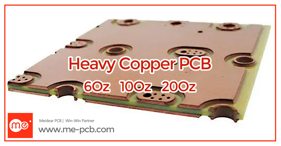
Today, Meidear PCB brings you an introduction to two Heavy Copper PCBs, both of which are 4-layer through-hole boards with copper thickness requirements of inner 6Oz and outer 6Oz, and inner 3Oz and outer 10Oz, respectively! Let's first take a look at what these two heavyweight players look like


Inner copper thickness 3Oz (>105um)
Outer copper thickness 10Oz (>350um)
microgram
10Oz / 3Oz / 3Oz/10Oz micro slicing Heavy Copper in shenzhen Meidear PCB

Inner copper thickness 6Oz (210um)
Outer copper thickness 6Oz (210um)
microgram
6Oz / 6Oz / 6Oz / 6Oz micro slicing Heavy Copper in shenzhen Meidear PCB
The circuit design of thick copper plates is generally relatively simple, but controlling the parameters during the manufacturing process is quite difficult
Material selection:
For 10Oz thick copper circuit boards, it is necessary to use high resin content semi cured sheets to ensure that the flow rate of interlayer semi cured sheets is sufficient to fill the inner layer graphics, while avoiding quality problems such as delamination and ineffective high-voltage testing caused by excessively thick or thin insulation layers in the finished board.
Compression production:
The copper thickness production of thick copper plates cannot be completed through electroplating and electrification like typical PCBs. The copper thickness of 10OZ is achieved by pressing 0.3mm copper plates on both sides of the core board, followed by electroplating and electrification. The pressing of copper plates is much more difficult than that of copper foils.
Drilling production:
When using high TG, high-speed, high-frequency, thick copper special plates, it increases the difficulty of drilling roughness, drilling burrs, and removing drilling stains. The cumulative total copper thickness and plate thickness of multi-layer boards make drilling tools prone to breakage and the problem of oblique drilling caused by plate thickness and copper thickness are both manufacturing difficulties.
Circuit production:
In circuit production, due to the thick copper foil, conventional etching methods are difficult to etch the complete circuit. Different factories have their own etching techniques for thick copper plates. We also adjust the process for different products, accurately control the etching depth and shape, and ensure the quality of the circuit and holes.
If you have any enquiries about our products (Heavy Copper PCB), or wish to get in touch with our staff, please feel free to contact us using the form below.
mkt@me-pcb.com
Whatapps:15914074643
Thank you!
Related News

How many types of surface treatment processes for PCB?
Sep .04.2024
PCB surface treatment processes
HASL,OSP ENIG,Immersion Silver,Immersion Tin hard Gold
nickel P-alladium gold
HASL,OSP ENIG,Immersion Silver,Immersion Tin hard Gold
nickel P-alladium gold
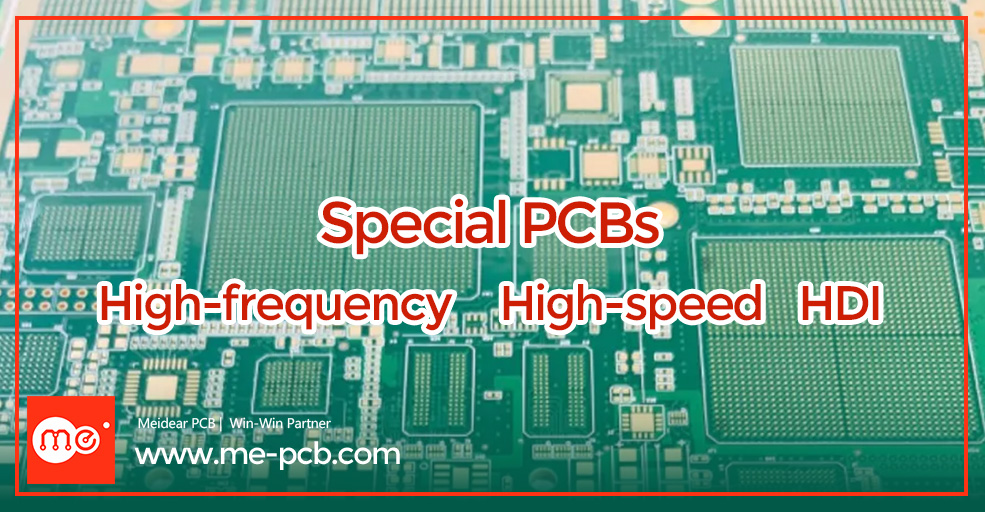
The material difference between high-frequency PCB and high-speed PCB
Sep .03.2024
Professional production, high-frequency, high-speed, HDI, LED lighting board, (Flex, Rigid-Flex,) (Wangling, Taiyao, Nanya, Isola, Rogers, Pana-sonic,) Quotation email: mkt@me-pcb.com

HDI LED lighting PCB in Shenzhen China Mepcb
Aug .08.2024
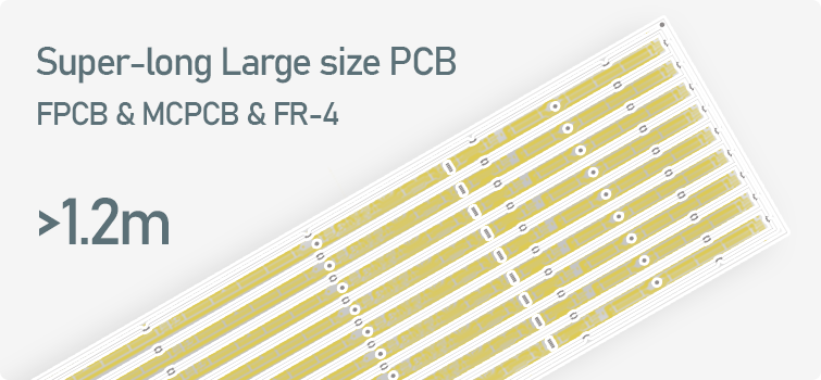
The most popular small spacing LED screen is like this
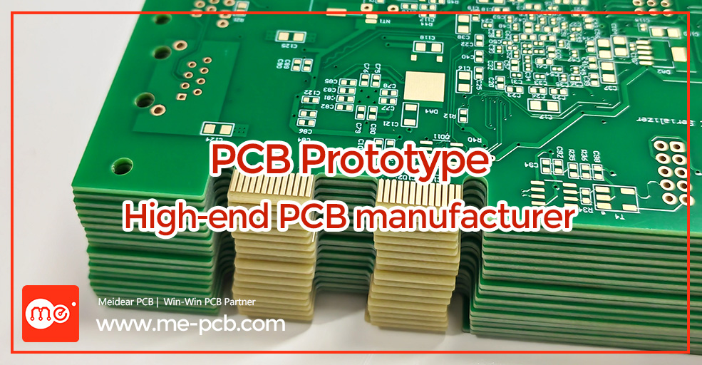
High-end Prototype Printed circuit board manufacturer in Shenzhen
Aug .22.2023
Meidear PCB | PCB and PCBA one-stop service provider
BGA and Gold finger PCB
EING 2U PCB
BGA and Gold finger PCB
EING 2U PCB