
How many types of surface treatment processes for PCB?
Views : 84
Author : Meidear
Update time : 2024-09-04 09:15:40
How many types of surface treatment processes for PCB?

Surface treatment is a very important in the manufacturing process of PCB (Printed Circuit Board).
Surface treatment can improve the solderability, corrosion resistance, and reliability of PCBs,
while also increasing the appearance quality of PCBs. According to different requirements, PCB surface treatment processes can be divided into various types. In this article, we will introduce several common PCB surface treatment processes and their characteristics.

There are many surface treatment processes for PCB circuit boards, including hot air leveling, organic coating (OSP), chemical nickel plating/immersion gold, silver deposition, tin deposition, etc.
1、HASL(Hot Air Solder Leveling) and HASL-LF(Lead-free)
Lead-free Hot Air Solder Leveling Process, also known as tin spraying, is a commonly used treatment process for early PCB boards. It involves coating the PCB with molten tin lead solder and leveling it with heated compressed air to form a coating layer that is both resistant to copper oxidation and provides good solderability. During hot air conditioning, solder and copper form a copper tin metal compound at the junction, with a thickness of approximately 1-2 mil.

2、OSP(Organic solderability preservative)
Organic Solderability Preservative (OSP) is an organic coating used to prevent copper oxidation before soldering, which protects the solderability of PCB pads from damage. The two widely used OSPs belong to nitrogen-containing organic compounds, namely benzotriazoles and imidazolium organic crystalline bases. They can all adhere well to bare copper surfaces and are very specific - they only care about copper and will not adhere to insulation coatings such as solder mask.
Triazine will form a molecular thin film on the copper surface. During the assembly process, when a certain temperature is reached, this thin film will be melted off, especially during reflow soldering, where OSP is more prone to volatilization. The protective film formed by imidazole organic crystalline base on copper surface is thicker than that of triazine, and can withstand more thermal cycles during assembly.
Triazine will form a molecular thin film on the copper surface. During the assembly process, when a certain temperature is reached, this thin film will be melted off, especially during reflow soldering, where OSP is more prone to volatilization. The protective film formed by imidazole organic crystalline base on copper surface is thicker than that of triazine, and can withstand more thermal cycles during assembly.

OSP process is different from other surface treatment processes as it acts as a barrier layer between copper and air; Simply put, OSP is the chemical process of growing an organic film on a clean bare copper surface. This layer of film has oxidation resistance, heat shock resistance, and moisture resistance, mainly used to protect the copper surface from further rusting in normal environments; At the same time, it must be easily removed by the soldering flux in the subsequent high temperature welding process for easy soldering. OSP technology is simple, cost-effective, and widely used in the production of circuit boards.
3、ENIG(Electroless Nickel and Immersion Gold)
Electroless Nickel and Immersion Gold (short for ENIG) is a process used for surface treatment of printed circuit boards (PCBs). During the PCB manufacturing process, the copper layer, due to its active chemical properties, is prone to oxidation in air, resulting in the formation of a non-conductive or poorly conductive oxide film on the surface of the solder pad. This will affect the quality of soldering, electrical performance, and long-term reliability.

Shenzhen Meidear
Professional production, high-frequency, high-speed, HDI, LED lighting board, (Flex, Rigid-Flex,) (Wangling, Taiyao, Nanya, Isola, Rogers, Pana-sonic,) Quotation email: mkt@me-pcb.com
The gold deposition process includes two main steps:
Chemical nickel plating: Firstly, a thin layer of chemical nickel is uniformly deposited on the exposed copper surface of the entire PCB. This nickel layer not only provides good corrosion protection, but also has good flatness, suitable for high-density packaging and fine pitch device applications.
Gold plating: Subsequently, a thin layer of gold is deposited on top of the chemical nickel layer. This layer of gold mainly covers the nickel layer, especially in the contact points and connector areas of the circuit board, such as gold fingers. Gold has excellent oxidation resistance, corrosion resistance, and excellent conductivity, which can ensure that the solder pads maintain good solderability and electrical connectivity for a long time.
The benefits of using the immersion gold process include providing excellent weldability and long-term stability. Reduce impedance mismatch and signal attenuation in signal transmission. Reduce the problem of poor tin consumption caused by oxidation. For high-frequency and high-speed circuit boards, signal loss and reflection effects can be reduced. It has good flatness and is suitable for fine assembly processes such as surface mount technology (SMT) and chip level packaging (CSP).
4、Immersion Silver
Chemical silver deposition, as a lead-free PCB surface treatment process, involves depositing a layer of silver with a thickness of 6-16 μ inches on the copper surface through displacement reaction. The surface is intact, with good conductivity and solderability.
Advantages:
Smooth surface, very suitable for SMD and BGA packaging;
Can replace electroplated nickel or chemically deposited nickel gold as the standard surface for aluminum and gold wire bonding;
Can replace electroplated nickel/silver as bonding wire and as a good reflective surface;
Good conductivity and can be used for contact conduction applications;
The min risk of electromigration and the small Jafani effect.

5、Immersion Tin
Chemical tin deposition is the most ideal process to replace tin spraying by changing the chemical potential of copper ions, causing a displacement reaction between Sn2+in the plating solution and the copper surface of the PCB board, resulting in a silver white tin layer with a thickness of about 1 μ m on the copper surface. The product is suitable for PCB boards with fine and dense wires, as well as Press fit insertion technology. It is suitable for lead-free mounting processes and can meet the requirements of multiple soldering; Suitable for horizontal and vertical tin deposition.

Advantages Introduction:
No electromigration effect, no dendritic growth of tin layer, effectively controlling tin whiskers;
Uniform surface color;
Good compactness and antioxidant properties;
Excellent PIM value stability.
6、Chemical nickel P-alladium gold
Compared with immersion gold, chemical nickel pall gold has an additional layer of pa between nickel and gold. Pa can prevent corrosion caused by displacement reactions and make sufficient preparations for immersion gold. Gold tightly covers pa, providing a good contact surface.
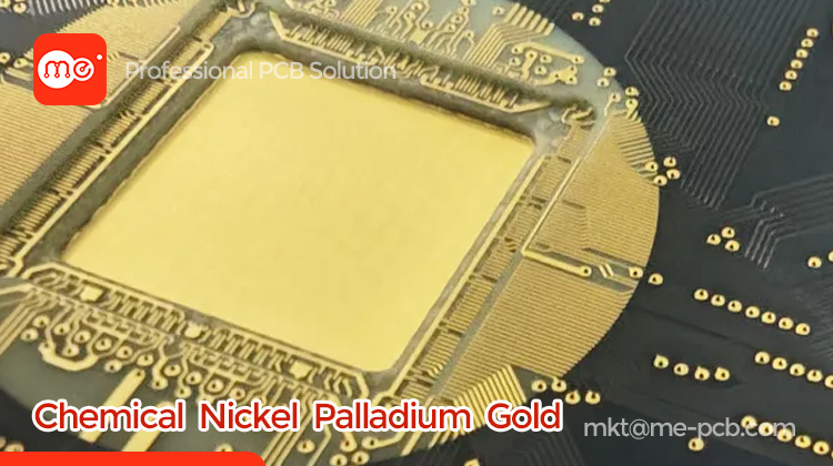
The surface treatment adopts nickel pall gold technology. The surface treatment of nickel pall gold has strong adhesion, is not easy to peel off, and improves the reliability and stability of the product.
Advantages:
Suitable for lead-free soldering. The surface is very smooth and suitable for SMT. Through holes can also be coated with nickel gold. Longer storage time and less demanding storage conditions. Suitable for electrical testing. Suitable for switch contact design. Suitable for aluminum wire binding, suitable for thick plates, strong resistance to environmental attacks.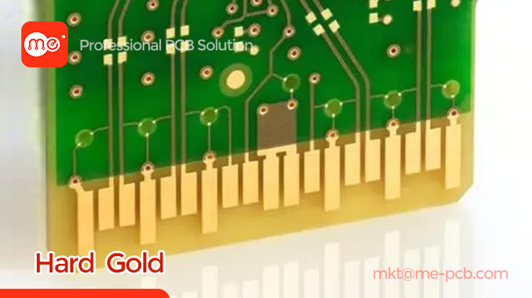
The changes in the surface treatment process of PCBs are not significant and seem to be quite distant, but it should be noted that long-term slow changes will lead to significant changes. With the increasing demand for environmental protection, the surface treatment process of PCBs will definitely undergo tremendous changes in the future.
We are professional LED PCB, FR4 PCB, aluminum PCB, flexible circuit boards Manufacturer.
Meidear is dedicated to manufacture quick turn prototype & samples, and small-medium volume quality PCBs. While we are dedicated to make your PCB sourcing job easy and reliable, with our efforts, experience and service.
you can drop mail to mkt@me-pcb.com for more information.

The surface treatment adopts nickel pall gold technology. The surface treatment of nickel pall gold has strong adhesion, is not easy to peel off, and improves the reliability and stability of the product.
Advantages:
Suitable for lead-free soldering. The surface is very smooth and suitable for SMT. Through holes can also be coated with nickel gold. Longer storage time and less demanding storage conditions. Suitable for electrical testing. Suitable for switch contact design. Suitable for aluminum wire binding, suitable for thick plates, strong resistance to environmental attacks.
7、Electrodeposited Au (Hard Gold)
In order to improve the wear resistance of the product and increase the number of insertions and removals, hard gold is electroplated.

The changes in the surface treatment process of PCBs are not significant and seem to be quite distant, but it should be noted that long-term slow changes will lead to significant changes. With the increasing demand for environmental protection, the surface treatment process of PCBs will definitely undergo tremendous changes in the future.
We are professional LED PCB, FR4 PCB, aluminum PCB, flexible circuit boards Manufacturer.
Meidear is dedicated to manufacture quick turn prototype & samples, and small-medium volume quality PCBs. While we are dedicated to make your PCB sourcing job easy and reliable, with our efforts, experience and service.
you can drop mail to mkt@me-pcb.com for more information.
Related News
The material difference between high-frequency PCB and high-speed PCB
Sep .03.2024
Professional production, high-frequency, high-speed, HDI, LED lighting board, (Flex, Rigid-Flex,) (Wangling, Taiyao, Nanya, Isola, Rogers, Pana-sonic,) Quotation email: mkt@me-pcb.com
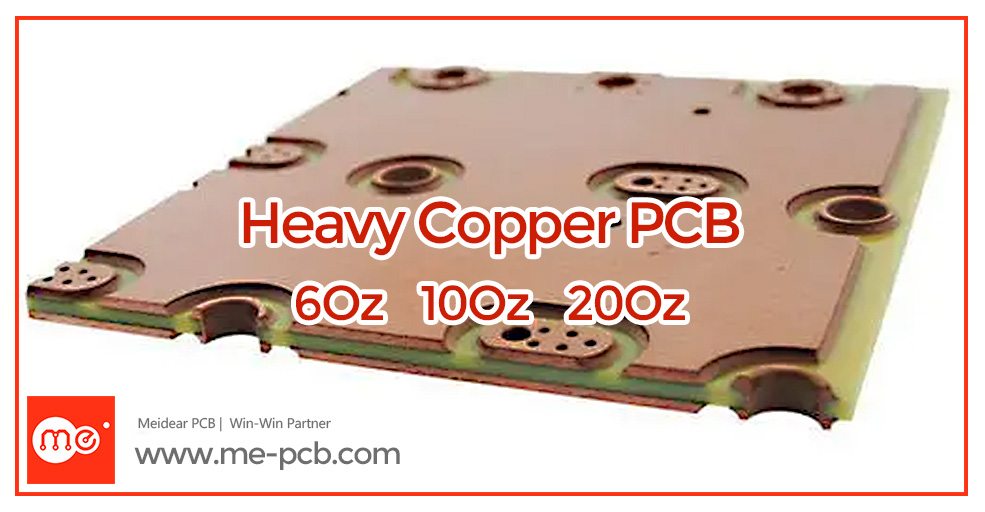
High-performance Thick copper heavy Copper PCB 6Oz 10Oz 20Oz
Aug .09.2024
Heavy Copper PCB 6Oz 10Oz 20Oz Multi-layer board
Professional customized production
in Shenzhen Shajin
Professional customized production
in Shenzhen Shajin

HDI LED lighting PCB in Shenzhen China Mepcb
Aug .08.2024
The most popular small spacing LED screen is like this
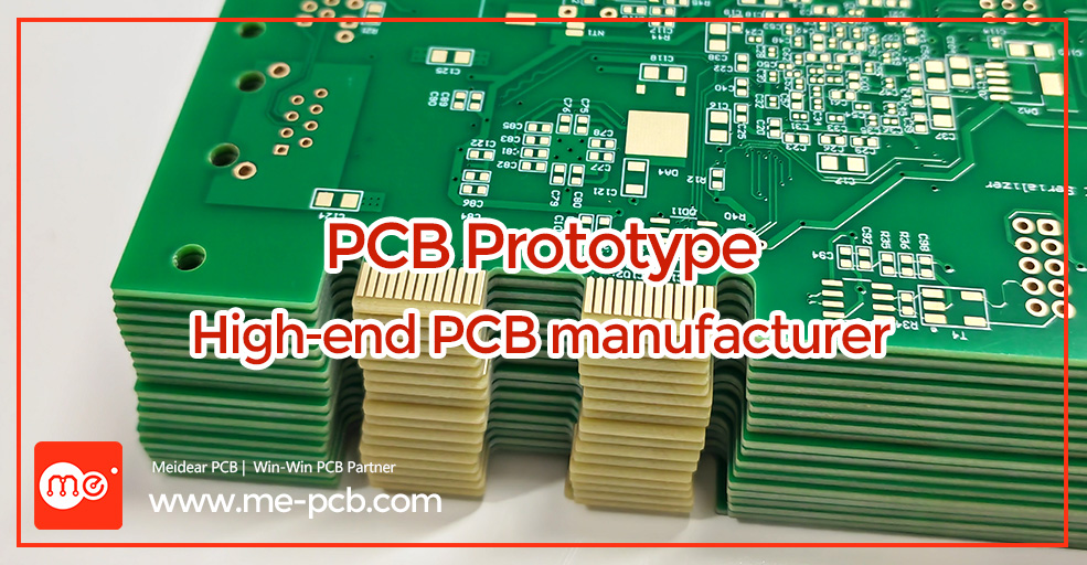
High-end Prototype Printed circuit board manufacturer in Shenzhen
Aug .22.2023
Meidear PCB | PCB and PCBA one-stop service provider
BGA and Gold finger PCB
EING 2U PCB
BGA and Gold finger PCB
EING 2U PCB